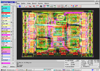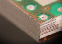
Our experts will help to develop the circuit diagrams of your devices (digital, analog and power circuitry), will make the tracing of printed circuit boards and prepare the documentation for production. If you already have produced your products, we can offer (if necessary) the technological redesign of your products in accordance with the requirements to modern automated assembly of printed circuit boards and reducing of the number of terminal components. It also allows you to reduce the range of used components and to optimize the delivery and reduce costs.
Unfortunately, in Russia a lot of developers (tracers) of PCB pay all their attention to placement of components taking into account only the factors affecting on availability of the product (minimizing connections shielded HF circuits, etc.) completely forgetting about the requirements for the topology of PCB in terms of modern automated assembly. Meanwhile, compliance with certain requirements for the arrangement of elements on a circuit board and conductors configuration let to avoid a lot of production problems, leading to increasing of the number of defective products.
We can offer companies already producing products and using domestic components to implement projects with import element base (with a maximum number of SMD components) with the same (or better) characteristics free of charge, if you decide to order a full cycle of manufacture from us.
Our experts, who were trained in overseas factories, are ready to advise your designers on issues related to adaptation of your project to the requirements of a modern assembly plant, the implementation of «hard copy» FPGA and the «silicon compilation». For our clients we can offer a unique service, as monitoring and early notification about the components that are discontinued, and included in the so-called “stop-lists”. This service will allow to redesign products in advance. In addition, it is possible to replace these components and redesign the project with our specialists if you need.

